High-power electronics are becoming ubiquitous across EV fast chargers, powertrains, solar inverters, data centers, and grid-scale power transmission systems. As current levels rise and operational voltages increase, even minor design discrepancies carry severe operational risks. Failures rarely remain localized to a single component—they often cascade across entire system architectures, causing operational downtime and severe safety hazards.
High-power electronics testing is designed to address this exact challenge. Rather than merely verifying basic circuit functionality, it quantitatively determines how power devices perform under high-voltage stress, heavy load currents, high switching frequencies, and extreme thermal conditions—simulating real-world operating environments far beyond nominal laboratory conditions.
IKAM delivers high-power electronics testing solutions in compliance with international standards, covering static parametric extraction, dynamic switching characterization, and both on-wafer probing and packaged power module testing.
Manufacturer datasheet specifications are typically derived under controlled, steady-state laboratory conditions. However, when deployed in real-world systems, power devices endure simultaneous high-voltage stress, heavy surge currents, rapid thermal cycling, and continuous high-frequency switching. The discrepancy between ideal test conditions and actual operating stresses is the root cause of late-stage design failures.
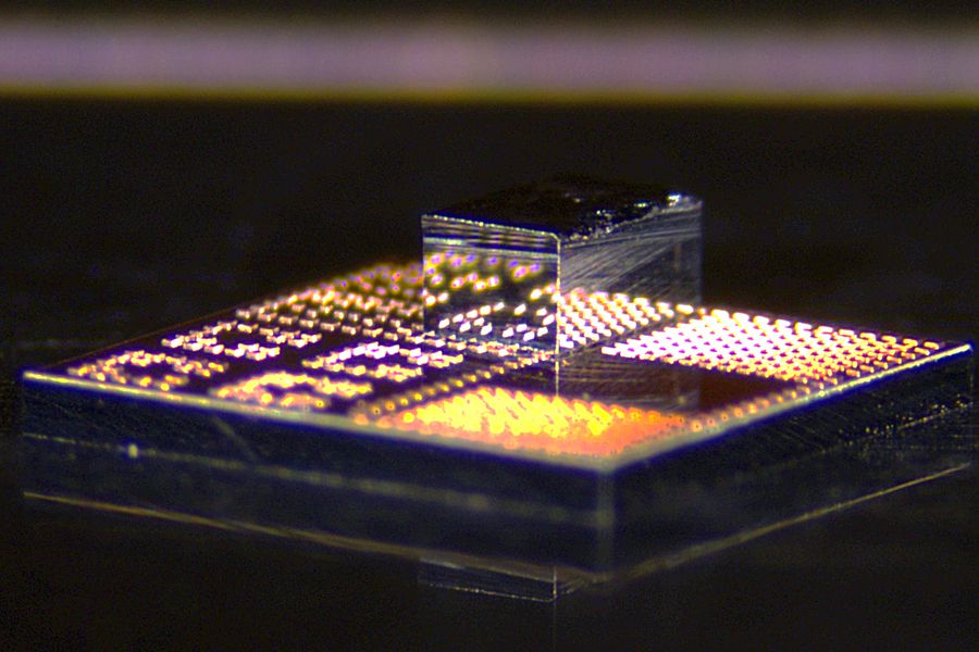
This challenge is amplified as the industry transitions from conventional Silicon to wide-bandgap (WBG) semiconductors like Silicon Carbide (SiC) and Gallium Nitride (GaN). These WBG devices offer faster switching speeds, reduced conduction losses, and smaller passive components (inductors and capacitors), yielding lighter systems with superior energy efficiency. Conversely, high switching speeds ($dV/dt$ and $dI/dt$) exacerbate self-heating, electromagnetic interference (EMI), and dynamic parameter drift—requiring testing methodologies specifically tailored to capture these WBG-specific behaviors.
The initial step in any characterization pipeline is static testing, which establishes steady-state current-voltage ($I-V$) relationships: threshold voltage ($V_{th}$), on-state resistance ($R_{DS(on)}$), off-state leakage current ($I_{leak}$), and breakdown voltage ($V_{BR}$). High-power parameter analyzers can measure from sub-picoamperes up to tens of kilovolts and thousands of amperes in a single platform, serving both low-power discrete devices and high-power IGBT, SiC, and GaN modules.
Beyond static $I-V$ metrics, parasitic terminal capacitances ($C_{iss}$, $C_{oss}$, $C_{rss}$) directly dictate switching losses and actual turn-on/off speeds. Many traditional labs rely on basic curve tracers that lack capacitance-voltage ($C-V$) measurement capabilities, leaving device characterization incomplete. Integrating $C-V$ profiling into static test systems resolves this diagnostic gap without requiring entirely separate instrumentation.

Static testing reveals only a fraction of a power device's performance profile. In actual power conversion topologies, devices switch continuously at high frequencies under high voltage and inductive loads, generating dynamic phenomena that static tests cannot capture: turn-on/off transition times, switching energy losses ($E_{on}$, $E_{off}$), dynamic $R_{DS(on)}$, gate charge ($Q_g$), and reverse recovery behavior.
Double Pulse Testing (DPT) is the industry-standard methodology for extracting these dynamic parameters in wide-bandgap semiconductors. By applying two sequential voltage pulses under real load conditions, DPT accurately captures switching transients before self-heating raises junction temperatures and skews data. Repeated pulse testing also exposes dynamic $R_{DS(on)}$ degradation over time—a characteristic behavior in GaN HEMTs undetectable via static DC measurements.
Evaluating power device switching behavior requires more than aggregated numeric metrics; it demands direct visualization of voltage and current waveforms during each switching cycle. Wide-bandwidth oscilloscopes paired with high-voltage differential and current probes reveal transient anomalies—such as inductive voltage overshoot, ringing, waveform distortion, and fast glitches—that summary data fails to capture.
High-speed pulse generators act as precision gate drivers, triggering devices under exact switching conditions with fast edge rates to simulate gate-drive signals in automotive and industrial power circuits. Combining these tools allows engineers to perform both quantitative measurements and real-time visual analysis of dynamic device behavior.
A versatile power electronics test platform serves multiple engineering roles within an organization: circuit designers require precise device models for component selection, incoming inspection engineers need rapid screening, failure analysis teams must isolate defect root causes, and semiconductor device developers require parametric feedback directly during fabrication.
On-wafer testing identifies parametric variations while die remain un-packaged, eliminating unnecessary packaging costs for defective die. Advanced high-voltage wafer probers execute parametric sweeps up to $3\text{ kV}$ in a single automated pass, integrating low-voltage and high-voltage test sequences into one seamless cycle rather than toggling between separate test stations—drastically increasing throughput in power wafer fabs.
The automotive sector represents the most stringent application for high-power electronics. Electric vehicle (EV) powertrains, onboard chargers (OBCs), and main traction inverters must operate reliably under harsh mechanical vibration, heavy EMI, and wide ambient temperature swings. Stricter emissions regulations and rapid EV adoption are driving widespread deployment of SiC and GaN devices, elevating testing rigor across the supply chain.
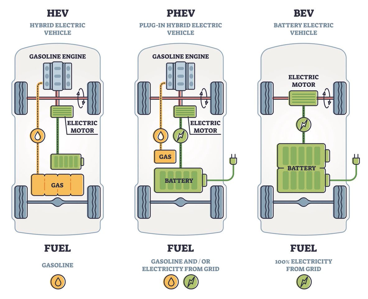
Automotive-grade test instrumentation covers measurement ranges spanning sub-nanoamperes to over $1,500\text{ A}$, and microvolts to $3\text{ kV}$—fully accommodating EV power semiconductors. Specialized dynamic current waveform analyzers detect transient load anomalies under real driving cycles, providing diagnostic depth that static DC testing cannot replicate.
Beyond individual components, programmable power supplies and electronic loads used in automated test equipment (ATE) lines must scale to higher power densities to match target device requirements. Modern testing architectures increasingly adopt regenerative power supplies capable of feeding absorbed load energy back into the local AC grid rather than dissipating it as waste heat—drastically reducing electricity costs and thermal loads within test facilities.
Modern programmable power systems deliver modular outputs from $1.5\text{ kW}$ to $12\text{ kW}$ per unit, achieving high power density up to $6\text{ kW}$ in standard rack form factors. This saves significant rack space compared to legacy equipment while maintaining high measurement accuracy and repeatability for multi-kilowatt device validation.
IKAM provides application-specific system configurations for high-power electronics testing—spanning power semiconductor R&D labs, wafer-level probing, EV power subsystem validation, and automated industrial manufacturing lines.